A junction diode is one of the most fundamental and widely used semiconductor devices in electronics. It is formed by joining two types of doped semiconductor materials—p-type and n-type—to create a pn junction. What makes this junction special is its ability to conduct current effectively in one direction while offering high resistance in the opposite direction. This unidirectional conduction makes junction diodes essential in rectification, signal processing, voltage regulation, and switching circuits.
At its core, a junction diode is built on the principle that different charge carriers dominate in different types of semiconductors. In an n-type material, electrons are the majority charge carriers, while in a p-type material, holes are the majority carriers. When these two materials are brought together, interesting physical and electrical phenomena occur at the junction that control the flow of current.
How Junction Diodes Are Manufactured
The process of manufacturing a junction diode begins with obtaining semiconductor material of the highest purity. Elements like silicon (Si) or germanium (Ge) are typically used, and these materials must have impurity levels lower than one part per billion to ensure the desired electrical behavior. The purification is usually achieved through a combination of chemical treatments and zone refining techniques. Once a highly pure polycrystalline form is obtained, it is transformed into a single crystal using either the Czochralski method or the Floating Zone technique. The single crystal is then sliced into thin wafers for further processing.
Two widely used technologies for creating junctions within these wafers are diffusion and epitaxial growth.
In the diffusion process, a p-type dopant such as boron is diffused into an n-type silicon wafer in a controlled, high-temperature environment. Initially, the wafer is oxidized to form a protective silicon dioxide layer. A masking technique is then used to selectively etch away portions of this layer to allow diffusion only in desired regions. The result is the formation of a pn junction beneath the wafer’s surface. This method is highly effective in planar technology, allowing for the precise creation of multiple diodes simultaneously with improved performance and scalability.
In contrast, epitaxial growth involves depositing semiconductor layers in vapor form over a heavily doped substrate (often referred to as n⁺ for heavy n-type doping). This method allows for layer-by-layer construction of semiconductors with exact control over electrical properties and crystal orientation. A base wafer acts as the support, and additional layers are grown on top. A p-region is later introduced by diffusion after selective masking. This approach is often used to build more complex and high-performance semiconductor devices.
Working Principle of a PN Junction
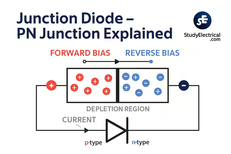
Once a junction is formed between p-type and n-type materials, the device exhibits fascinating behavior due to the interaction between electrons and holes near the junction. Because electrons dominate the n-side and holes dominate the p-side, a process known as carrier diffusion occurs immediately after the junction is formed. Electrons migrate into the p-region and combine with holes, while holes migrate into the n-region and recombine with electrons. These recombinations create fixed negative ions on the p-side and fixed positive ions on the n-side, leaving behind a region devoid of any free carriers. This area is called the depletion region.
The depletion region acts as a barrier to further movement of carriers. An internal electric field forms due to the fixed charges, and this field creates a contact potential (denoted as V0), typically in the range of a few tenths of a volt. This potential opposes the flow of additional majority carriers across the junction. However, a small equilibrium current is maintained by minority carriers (electrons in the p-region and holes in the n-region), which are thermally generated and driven by the internal electric field.
Diode Biasing Conditions
When a voltage is applied to the diode, the direction of the applied bias—forward or reverse—determines how current will flow through the device.
In reverse bias, the positive terminal of a battery is connected to the n-side (cathode), and the negative terminal is connected to the p-side (anode). This causes majority electrons and holes to move away from the junction, further widening the depletion region. The internal potential barrier increases to V0 + V, which effectively blocks the flow of majority carriers. Only a small reverse current flows, caused by minority carriers. This current is called the reverse saturation current (Is). Its value is extremely small—typically in the nanoampere range for silicon diodes—and remains nearly constant until the diode reaches breakdown voltage.
In forward bias, the polarity is reversed—the positive terminal is connected to the p-side, and the negative to the n-side. This reduces the potential barrier to V0 − V, allowing majority carriers to easily cross the junction. The result is a large current flow, known as forward current (If).
You can explore this topic further in our dedicated article on Forward and Reverse Bias of PN Junction Diode.
I-V Characteristics of a Junction Diode
The current-voltage relationship of a diode can be expressed mathematically using the diode equation:
I = Is (eeV/ηkT - 1)At room temperature, this equation simplifies to:
- For germanium: I = Is (e40V – 1)
- For silicon: I = Is (e20V – 1)
Silicon diodes require a forward voltage of about 0.7 V (threshold voltage) to conduct significantly, while germanium diodes begin conducting around 0.3 V. The reverse saturation current in germanium is higher and doubles for every 10°C rise in temperature.
At high reverse voltages, the junction may experience breakdown, where current increases dramatically. This is used in Zener diodes for voltage regulation.
Applications of Junction Diodes
Junction diodes are used in various electronic circuits. Common applications include:
- Rectifiers for converting AC to DC
- Voltage regulators using Zener diodes
- Switching circuits
- Clipping and clamping circuits
- Signal detection and waveform shaping
FAQs – Junction Diodes
1. What is the function of a junction diode?
It allows current to flow in one direction (forward bias) and blocks it in the other (reverse bias), making it ideal for rectification and signal control.
2. Why doesn’t a diode conduct in reverse bias?
In reverse bias, the depletion region widens and the barrier potential increases, blocking the majority carriers and allowing only a very small minority carrier current.
3. What is the depletion region?
A region around the junction where mobile carriers are depleted, leaving behind immobile ions that create an electric field and a potential barrier.
4. What is forward current?
It is the large current that flows when a diode is forward biased and the barrier potential is reduced, allowing majority carriers to cross the junction.
5. Where can I learn more about diodes and electronics?
Visit our Electronic Devices and Circuits section for comprehensive tutorials and diagrams.
Conclusion
The junction diode is a cornerstone of electronic circuit design. Its ability to control the direction of current flow, respond to voltage changes, and act as a rectifier or regulator makes it indispensable in both analog and digital electronics. Understanding how the pn junction works, and how the diode behaves under various biasing conditions, is crucial for anyone pursuing electrical or electronic engineering.