The problem of storing charge in a pn-junction can be solved in a Schottky diode. This is done by creating a “barrier potential” with a metal-semiconductor contact. A layer of metal is put on a thin layer of n-type silicon. This barrier acts like a pn-junction.
The diode works based on majority carriers only, so there are no extra minority carriers to combine. When the diode recovers, it’s because of its own capacitance. The recovered charge in a Schottky diode is much less than in a pn-junction diode. This is because it’s only due to the junction capacitance and doesn’t depend much on the reverse di/dt. Schottky diodes have a low forward voltage drop.
However, the leakage current of a Schottky diode is higher than that of a pn-junction diode. When a Schottky diode has a low conduction voltage, it has a high leakage current, and the other way around. So, these diodes are usually used for low voltages, up to around 100V. They can handle currents from 1 to 400 A. Schottky diodes work well in high-current, low-voltage DC power supplies. They’re also used in low-current power supplies to save energy.
Operating Principle and Structure of Schottky Diode
The operational principle of the Schottky power diode is based on the interaction between a metal and a depleted layer of a semiconductor, and the contact between which has rectifier properties in certain conditions.
Schottky diodes are based on n− silicon with electron conductivity. The highly doped n+ substrate has a donor concentration of 5 × 10¹⁸ – 5 × 1019 cm−3 and its thickness is 150–200 μm; this is determined by the thickness of the initial silicon plate.
The presence of a highly doped substrate considerably reduces the resistance of the diode and ensures satisfactory ohmic contact with the metallized cathode layer.
The active n– base of the Schottky diode has a lower impurity concentration (3 × 1015 cm−3). Its thickness WB is determined by the diode’s working voltage and is in the range from a few microns to tens of microns.
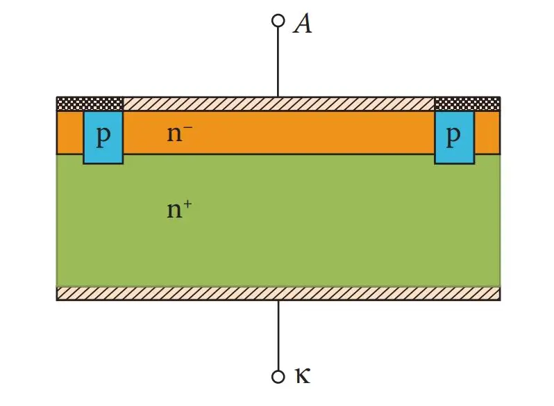
To minimize extreme avalanche breakdown and to increase the electric field strength in the base, the diode includes a system of guard rings with a p−n junction, whose depth is a few microns.
The voltage drop at the junction in the Schottky diode is less than that for a diode with a p−n junction, whereas the reverse currents are greater .
The forward voltage in the Schottky diode consists of two main components:
- the voltage at the junction and
- the voltage at the active-region resistance in the n− base of the diode.
$$U_F=\varphi_T \ln \left(\frac{I_F}{I_S}+1\right)+\frac{I_F \rho_n w_B}{S}$$
With an increase in the maximum reverse voltage of the Schottky diode, the resistance of the n− base increases, as the creation of higher reverse voltage requires a more extended weakly doped region with lower charge-carrier concentration.
As a result, the resistance of the n− base in high-voltage Schottky diodes is significantly increased. This is the main reason for the upper limit of 200–400 V on the working voltage of such diodes.
Related posts:
 Ideal and Typical Power Switching Waveforms
 Miniature cells and Batteries – Silver Oxide, Mercury and Lithium Cells
 Open Loop and Closed Loop Control System (4 Practical Examples Included)
 Introduction to PCB Assembly Process
 What is an Electrical Fuse? Types, Properties, and Application
 Digital Multimeter: Working and Application
 Understanding Passive Components in Electrical Engineering
 How Can I Find Work in FPGA?
 Top Educational Resources and Software for Understanding Electrical Machines
 Types of Power Electronic Converters