Electromagnetic interference (EMI) in printed circuit board (PCB) designs is a potential issue that can negatively impact the efficiency and integrity of electronic devices.
EMI can cause devices to malfunction, leading to data loss, signal degradation, and system failures. The chances of this issue occurring increase as devices become more compact and in demand to operate at higher frequencies. Thus, mitigation is a greatly needed aspect of PCB design.
As electronic devices become more compact and operate at higher frequencies, the potential for EMI increases, making its mitigation an essential aspect of PCB design.
Sources and Impacts of EMI
EMI can originate from various sources, both internal and external to the electronic device. Internal sources include clock signals, power supplies, and high-speed digital circuits, while external sources can be as varied as other electronic devices, power lines, and atmospheric disturbances. The impact of EMI on electronic devices can range from minor annoyances, like audio buzz and screen flickers, to critical failures in sensitive equipment, underscoring the need for effective EMI mitigation strategies.
Grounding and Shielding Techniques
Grounding and shielding represent the first line of defense against EMI. A well-implemented grounding strategy stabilizes the device’s electrical environment, providing a path for electromagnetic noise to dissipate safely. Shielding, meanwhile, involves enclosing sensitive parts of the PCB assembly in conductive or magnetic materials to create a barrier against external EMI sources. Effective shielding not only protects the device from incoming EMI but also prevents the device from emitting disruptive electromagnetic energy.
PCB Layout Considerations
The layout of a PCB plays a crucial role in mitigating EMI. Strategic placement of components, careful routing of signal and power traces, and the use of multiple ground planes can significantly reduce EMI emissions and susceptibility. Designers must pay particular attention to high-speed signal paths, ensuring that traces are short and direct to minimize the potential for EMI generation. Separating analog and digital components and incorporating filter circuits at key interfaces further enhances EMI mitigation.
Component Selection and Placement
Selection of the right components and their placements on the PCB is essential for reducing EMI. Components such as decoupling capacitors, which filter out high-frequency noise from power lines, and ferrite beads, which suppress high-frequency EMI on signal lines, are critical for maintaining signal integrity. Careful placement of these components, close to their associated ICs, maximizes their effectiveness in EMI suppression.
Advanced Manufacturing Techniques
Advancements in PCB manufacturing technology offer new opportunities for EMI mitigation. Techniques like controlled impedance routing and embedded passives allow for more precise control over the electrical characteristics of the PCB, reducing the likelihood of EMI issues. Additionally, the use of materials with favorable electromagnetic properties, such as low-dielectric-constant substrates, can help in minimizing EMI emissions and susceptibility.
Testing and Compliance
Testing for EMI compliance is a critical step in the PCB design process. Regulatory standards, such as those set by the FCC in the United States and the CE mark in Europe, establish limits for EMI emissions. Rigorous testing, including radiated and conducted emissions tests, ensures that the PCB meets these standards, avoiding expensive redesigns and delays in launching the product to market.
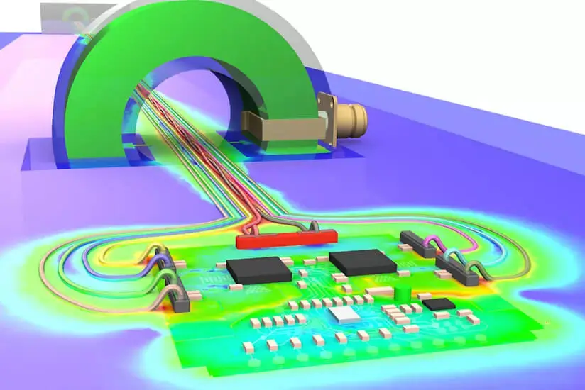
The Role of Simulation in EMI Mitigation
Simulation tools play an invaluable role in identifying potential EMI issues early in the design process. Electromagnetic simulation software can model how electromagnetic fields interact with the PCB and its environment, allowing designers to identify problem areas and test mitigation strategies without needing physical prototypes. This not only speeds up the design process but also leads to more effective EMI mitigation solutions.