Electronic products that are compact and up to date do not call for the traditional, more densely packed PCB.
To power the device without significantly lowering its performance, you will need a significantly more compact solution. And you can only accomplish this by utilizing an HDI printed circuit board.
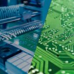
What exactly is an HDI PCB
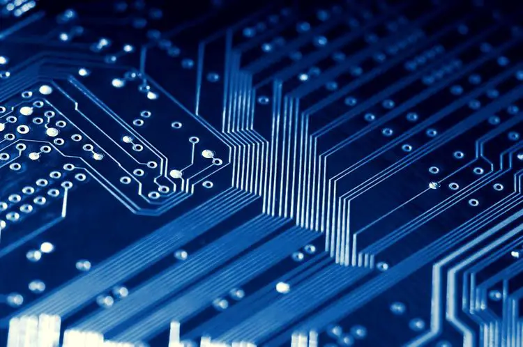
HDI PCB, which stands for high-density interconnected printed circuit board, is a connection of circuits that are interconnected to one another. Because of this, HDI PCB boards require a significantly smaller amount of surface area than standard PCB boards.
The amount of space between components has also been significantly reduced, contributing to improved heat dissipation.
The HDI PCB boards have been developed specifically for use in home appliances that require a robust PCB structure and have size restrictions.
Military-grade applications, digital cameras, cellular phones, touch devices, smart devices, and Internet of Things communications technologies like 4G and 5g all use the HDI PCB boards to get brilliant performance while conserving space. Examples of these types of applications include:
Mobile phones and cellular phones, touch-screen devices, laptop computers, digital cameras, 4G and 5G network communications, and various military applications, including avionics and intelligent munitions, are all examples of products that utilize this technology.
The HDI PCB improves the signal strength while also transforming the PCB boards’ overall executions.
The fact that HDI PCB boards use the blind vias and buried vias technology, both of which can be infused or integrated into micro vias, distinguishes them from other boards.
The HDI PCBs Have Many Valuable Advantages
It enhances the signal’s ability to be retained.
The HDI utilizes the blind via and via-in-pad technologies printed circuit board. And with this technology, you can place the components closer to one another, which ultimately shortens the signal’s path. Because of the shorter signal path, HDI PCB boards have improved signal retention.
Superb adaptability in all aspects.
The HDI PCB doesn’t pull its punches in the least bit when it comes to adaptability. It is the most exciting aspect of the board.
Having technologies such as blind via and via-in pad brings the components of the board much closer together, which in turn makes the board relatively compact. This allows the board to be incorporated into extensive and complex applications without sacrificing the product’s level of quality.
The increased service life of the PCB
You can use the HDI PCB for a more extended period because it has a less thermal expansion, which ensures that it will not fail due to higher temperatures.
This, in turn, means that you can use the HDI PCB for a more extended period, which ultimately extends the life of your device and improves its overall health.
A lower rate of heat conduction
Because the components in an HDI PCB are very close to one another, the heat transferred between them is also reduced to a minimum. This is because there is a shorter distance over which heat can travel.
Reduces the amount of time needed for production.
Because HDI PCBs have closely related components, their density is relatively lower than that of conventional PCB boards. This contributes to a reduction in the cost of manufacturing HDI PCBs.
This indicates that your company can supply more HDI PCB products instead of conventional ones.
You can get them here.
Takeaway
The best applications for HDI PCB boards are those that require less space but do not want to compromise on performance. This type of board improves performance while reducing the amount of space required.
The HDI PCB boards guarantee improved device communication thanks to their increased capacity for signal retention.