PCB assembly is the process of assembling electronic components on a Printed Circuit Board (PCB). In this article, you will learn the PCB assembly process and its equipment in general. By the end of the article, you will learn how the modern-day PCB assembly process happens in a big PCB manufacturing companies like NextPCB.
In today’s digital age, electronic products such as personal computers, mobile phones, and audio-video equipment cannot work without the application of the printed circuit board (PCB).
A PCB in these electronic products consists of a pattern of electrical traces etched from copper. It is laminated on an insulated base, which is typically rigid fiberglass.
PCB Assembly Process
The PCB serves as the interconnection device with electrical currents traveling on the board and the different discrete electronic components that are essential to the functioning of the electronic product.
We can assemble a few hundred to some thousand components on a single PCB.
PCB assembly is the process of assembling these electronic components on a Printed Circuit Board.
Three Types of PCB Assembly
Generally, PCB assembly is of three categories:
- Through-hole technology
- Surface-mount technology (SMT).
- Mixed Technology
1. Through-Hole Assembly
Through-hole technology is the simplest PCB assembly method. As a traditional PCB assembly method, the thru-hole mounting process is a combination of manual procedure and automatic procedure.
Through-hole technology works well on components with leads or wires that have to be mounted on board by plugging them through holes on board.
We apply through-hole technology for products where overall board size is not a significant concern.
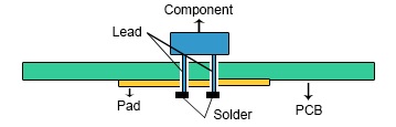
We insert the components into the holes drilled through the PCB. Finally, we solder the connections on the underside of the PCB between the component lead and the PCB pad.
2. SMT Technology
However, requirements from consumers, such as smaller product size and higher function and reliability, have forced the SMT (Surface-mount technology) to replace the Through-hole technology.
The configuration and the size of surface mount components have permitted mounting a large number of elements on a single PCB.
SMT PCB Assembly Process
The PCB assembly process in the SMT environment consists of five operations.
Step 1
First of all, the solder paste is applied where the components will be placed. Typically, it is applied by screen printing.
Step 2
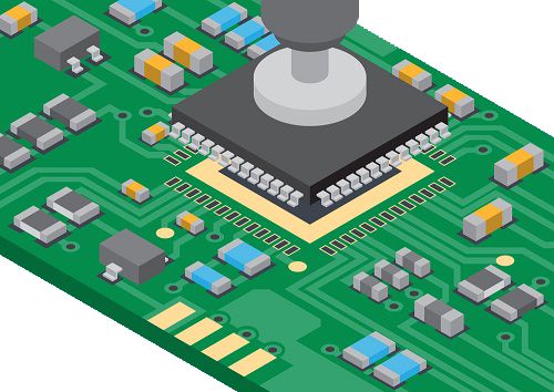
Next is the placement operation. A high-speed placement machine mounts small components such as chip resistors on the PCB first. Then a flexible placement machine installs larger components such as integrated circuits (ICs) on the PCB.
Step 3
After assembling all the components, the PCB is inspected for missing parts.
Step 4
Subsequently, the PCB is conveyed through an oven, which makes the solder paste reflow and forms the solder joints.
Step 5
Finally, the PCB must be cleaned to remove the contaminants exposed during fabrication and PCB assembly.
Single-Sided and Double Sided PCB
The PCB assembly line described above can be referred to as a single-sided assembly. That is, it is about PCBs that need mounting on one side.
On the other hand, the assembly line must be redesigned if the PCBs need double-sided mounting. For that, more additional placement machines are required to mount the components on the other side of the PCB.
3. Mixed Technology
Mixed technology is the combination of both Through-hole and surface mount technology.
With the advancement of modern science and technology, electronic products are becoming increasingly complex. Most of these circuit boards carry Through-hole components and SMD components, which require the collaboration of thru-hole technology and surface mount technology. This leads to mixed technology.
PCB Assembly Equipment
There are mainly two types of placement machines in the SMT environment. Each type of device possesses its peculiarities as well as the operation.
The two types of placement machines are
- Sequential pick-and-place (PAP) machine.
- Concurrent chip shooter (CS) machine
Sequential PAP Machine
The first type of PCB assembly placement machine is a sequential pick-and-place (PAP) machine.
In this type of machine, components of the same type are stored in a single stationary feeder, whereas the PCB is secured on a fixed working table.
During the placement operation, the assembly head travels to pick up one component at a time from a feeder and then places it on the stationary board.
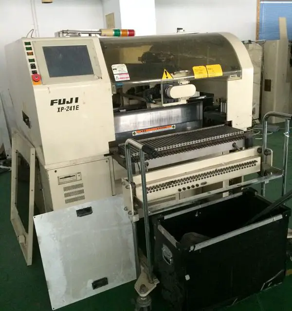
The PAP machine can achieve high accuracy. Moreover, it is suitable for operating with large components such as ICs. The Fuji XP-241E machine belongs to this category.
Concurrent chip shooter (CS) machine
The second type of machine is the concurrent chip shooter (CS) machine.
It possesses an X-Y table carrying a PCB, a feeder carrier with several feeders holding components, and a rotary turret with multiple assembly heads to pick up and place components.
Each assembly head has several nozzles of different sizes. A large nozzle is used to pick up and place large components.
The main advantage of the CS machine is its high speed because it performs the pickup and placement operations concurrently.
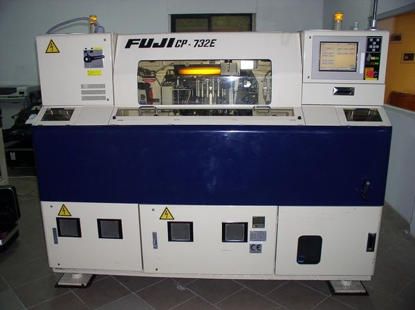
However, it is only preferable for operating with small components such as chip resistors. Because the placement of smaller components has priority, this type of machine is before the PAP machine in the assembly line. The Fuji CP-732E machine belongs to this category.
Although both the PAP machine and the CS machine are SMT placement machines, the configurations, as well as the characteristics of both devices, are different.
PCB Assembly Problems
PCB assembly planning consists of seven decision problems, which can be classified into two closely related issues:
- Setup management
- Process optimization
Setup management
- Line assignment: assigning board types to assembly lines;
- Machine grouping: grouping placement machines;
- PCB grouping: grouping PCBs into families;
- PCB sequencing: sequencing the production of PCBs.
Process optimization
- Component allocation: allocating component types to placement machines; x Component sequencing: determining the sequence of component placements;
- Feeder arrangement: assigning component types to feeders at each device.
Among the five assembly operations, component placement is generally the most time-consuming. Also, it is frequently a bottleneck in an assembly line and determines the line cycle time.
Due to the large production volumes, a minor reduction in cycle time will save significant production time.
Example
For example, to produce 50,000 boards, a reduction of six seconds in cycle time will save 5,000 minutes, that is, more than 80 working hours.
Therefore, to increase the efficiency or minimize the cycle time of the line, the component placement process must be optimized.
Modern PCB Assembly in NextPCB
NextPCB is one of the most experienced PCB manufacturers in China. They are specialized in the PCB assembly industry for over 15 years. They provide some of the most innovative printed circuit boards with assembly technologies in terms of the highest quality standards.
NextPCB was founded in 2004 and has since established itself as a turnkey PCB manufacturing and assembly factory for prototype quantities as well as small-volume to big-volume production.
PCB Assembly Types in NextPCB
NextPCB has professional PCB assembly capabilities in the following types.
- Surface Mount (SMT) Assembly
- Ball-Grid-Array (BGA) Assembly
- Mixed technology (SMT & Thru-hole)
- Through-Hole Assembly
- Mixed Assembly
- Kit Assembly
Through-hole assembly, SMT, and Mixed technology are explained in previous sections.
A ball grid array (BGA) assembly is a type of surface-mount assembly used for integrated circuits. BGA assembly is used for permanently mounting devices such as microprocessors. The Ball Grid Array has become increasingly popular for SMD ICs that require high-density connections.
Mixed Assembly – Through-Hole, SMT and BGA components are housed on the PCB.
NextPCB Quick Turnkey PCB Assembly Service
What is Turnkey PCB Assembly?
‘Turnkey’ refers to a product or service that is ready for immediate use for the buyer and when applied to PCB assembly. This means that the supplier (NextPCB) will handle all aspects of the PCB project.
This includes sourcing all the components, PCB manufacturing, PCB assembly, testing, and final shipment.
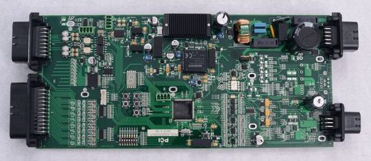
NextPCB has its own PCB Assembly manufacturer with 8 production lines to provide professional PCBA service and competitive prices for its customers.
PCB Assembly Process in NextPCB
NextPCB provides efficient and high-quality turnkey PCB assembly service to its customers. The PCB assembly process in NextPCB is explained below.
- Components Checking
- Solder Paste Printing
- Pick & Place SMD Parts
- Reflow Soldering
- Flipping
- Pick & Place SMD Parts
- THT Components Placement
- Wave soldering (hand soldering)
- AOI Checking/X-Ray
- Visual Inspection (Repairing)
- QC/Package
- Delivery
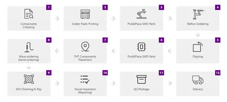
The main steps in the PCB assembly process in NextPCB are briefly explained below.
Components Checking
An incoming inspection, also known as a receiving inspection or material inspection, validates the quality of purchased raw materials based on set acceptance criteria.
It is performed by quality assurance personnel in the manufacturing facility to resolve quality issues during pre-production. Incoming inspection results follow an identification tagging system to determine required actions when an item is tagged as accepted, conditionally accepted, or rejected.
NextPCB team will do a full check on incoming material inspection to control the assembly quality. Components counting, package confirm, quantity confirm are in this process.
Solder Paste Printing
Solder paste (or solder cream) is a material used in the manufacture of printed circuit boards to connect surface mount components to pads on the board.
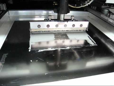
Before soldering, all PCB boards should print solder paste so that the components can be soldered by pick & place machine.
Pick & Place Assembly
Once bare PCBs printed solder paste, we move them to NextPCB’s automated Pick & Place machines for the actual mounting of components on their associated pads.
Component placement is 100% machine automated for maximum accuracy and efficiency and uses the project’s Centroid file for component coordinates and rotation data.
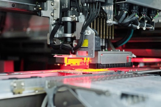
The boards are again inspected after components have been mounted to ensure all placements are accurate before the soldering process begins.
This stage might need to be performed multiple times, depending upon the specifics of a given project.
Double-sided SMT boards require one round of placement for the top and one for the bottom. Projects requiring wave soldering due to a high number of through-hole parts will typically have their components machine-placed as well.
Reflow Soldering
With parts mounted securely in place with solder paste underneath their pads, it is time for the PCBs to enter the reflow soldering oven.
Reflow Soldering is the most common method for PCB assembly in the industry today since it is much more flexible in terms of PCB layout requirements compared with the wave or hand soldering.
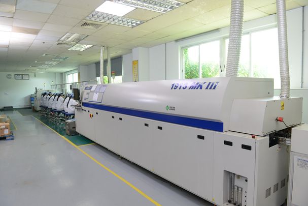
Most of the time, NextPCB can use reflow soldering for a majority of the parts on a circuit board. Then we pass the mostly-assembled boards to our highly skilled hand soldering team for the final few connectors and through-hole components. NextPCB has more than 6 reflow oven in its plant.
For double-sided assembly projects, the boards will need to be reflowed once for each side. A special adhesive is applied underneath the components that were soldered in the first run to prevent them from detaching and falling off the board when their solder is re-heated.
AOI (Automated Optical Inspection) Checking
After Reflow oven soldering, NextPCB will put the assembly board to an AOI machine. It is an automatic optical inspection machine to check quality for pick and place components.
This process is checking that the pin connected with pads is correct or not, the tin on the pads is over or not, etc.
X-Ray Inspection
After a reflow oven process, any boards including BGA, QFN, or other lead-less package types are sent for X-Ray Inspection.
This service is included by default on all NextPCB quotations which include such parts.
Wave Soldering
Wave soldering is a large-scale soldering process by which electronic components are soldered to a printed circuit board (PCB) to form an electronic assembly.
The name wave soldering is derived from the use of waves of molten solder to attach metal components to the PCB. It is for Through-hole components soldering.
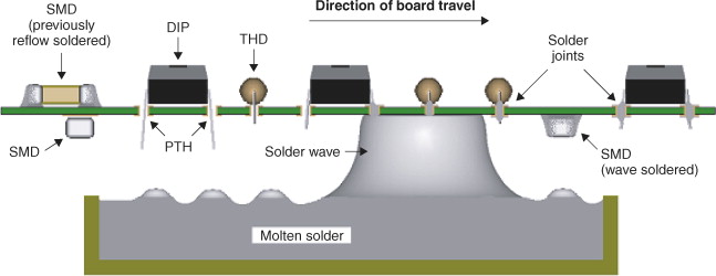
Normally if your order is small, it will not be soldered by wave soldering machine. If you insist, an extra fee will be added.
Quality for Every Stage of PCB and assembly in NextPCB has been controlled. In the PCB assembly process, it has Initial Sample Inspection, Defective Analysis, Functional Repairing, etc to control your PCBA projects to be high quality.
NextPCB Assembly Capabilities
| Assembly Types | Surface Mount (SMT) Assembly
Ball-Grid-Array (BGA) Assembly Mixed technology (SMT & Thru-hole) Through-Hole Assembly Mixed Assembly Kit Assembly |
SMT Parts Presentation | Cut tape
Partial reel Reel Tube Tray Laser-cut stainless steel |
Components Sourcing | Full turnkey (All components sourced by NextPCB)
Partial turnkey Kitted/Consigned |
|---|---|---|---|---|---|
| Component Types | BGA 0.25mm pitch with X-ray testing
Passive components as small as 01005 (0402)package Fine-pitch components as small as0.38mm pitch Hard metric connectors Cable & Wire Bulk |
Quality Inspection | Visual inspection
AOI checking BGA placement – X-RAY checking In-Circuit Test Functional test |
Others | Assembly Time:From 24 hours to 7days once all parts are ready
Max. Board Size: MOQ:5 pieces |
| Board Types | Rigid PCBs, Flexible PCB, metal core PCBs, Rigid-Flex PCBs |
Solder Types | Lead-Free (RoHS compliant) | ———— | ———— |
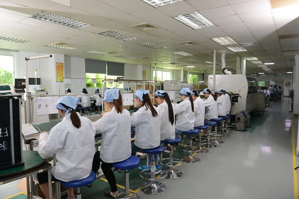
NextPCB Assembly Factory
NextPCB has a large assembly plant that has 6 SMT lines. It accepts min. order of 5 pcs and turnkey PCB Assembly services.
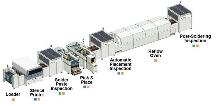
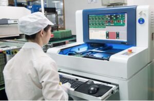
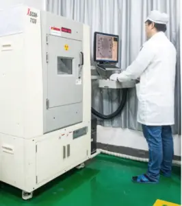
The above image shows the layout of an SMT assembly line. Some of the images of the NextPCB assembly factory is are displayed below.
How to place a PCBA order on NextPCB
Finally, we finished learning PCB assembly process. Its time to order your first PCB assembly from NextPCB. In this section, I will help you how to order your first PCB assembly from NextPCB.
Step 1: Go to the PCB Assembly Quote Form
Step 2: Three options are available – Turnkey, Knitted, and Combo. For Turnkey NextPCB will supply the parts. For knitted you have to supply the parts and for the combo you supply some and rest will be done by NextPCB.
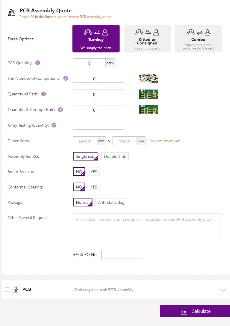
Step 3: Select the PCB quantity. A minimum of 5 quantities is required.
Step 4: Mention the Number of Components, Quantity of Pads, Quantity of Through Hole, X-ray Testing Quantity.
Step 5: Next enter the dimension of your board. The minimum dimension is 50mm*50mm.
After entering the remaining details you can successfully calculate the quoted amount for your PCB assembly work.

Comments are closed.