Solid state materials can be classified into three groups:
- insulators,
- semiconductors
- conductors.
Insulators have no free charge carriers available with them under normal conditions.
Conducting materials have plenty of free electrons available for electric conduction.
A semiconductor material is one whose electrical properties lie in between those of insulators and good conductors.
- Insulators are materials having an electrical conductivity less than 10-8 S/cm (like diamond: 10-16 S/cm);
- semiconductors have a conductivity between 10-8 S/cm and 103 S/cm (for silicon it can range from 10-5 S/cm to 103 S/cm );
- at last conductors are materials with high conductivities, greater than 103 S/cm :(like silver: 106 S/cm.)
The electrical conduction properties of different elements and compounds can be explained in terms of the electrons having energies in the valence and conduction bands. The electrons lying in the lower energy bands. which are normally filled. play no part in the conduction process.
Insulators
Stated simply, insulators are those materials in which valence electrons are bound very tightly to their parent atoms, thus requiring a very large electric field to remove them from the attraction of their nuclei.
In other words, insulators have no free charge carriers available with them under normal conditions.
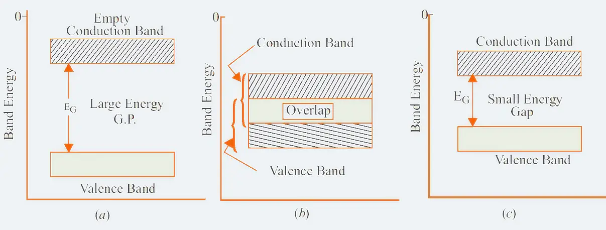
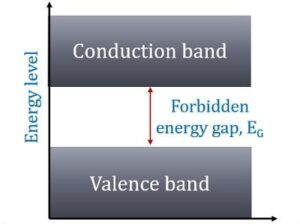
In terms of energy bands, it means that insulators [Fig(a)] have a full valence band,
- have an empty conduction band,
- have a large energy gap (of several eV) between them and
- at ordinary temperatures, the probability of electrons from full valence band gaining sufficient energy so as to surmount energy gap and thus become available for conduction in the conduction band, is slight.

This is shown in Fig(a). For conduction to take place, electrons must be given sufficient energy to jump from the valence band to the conduction band.
Increase in temperature enables some electrons to go to the conduction band which fact accounts for the negative resistance temperature coefficient of insulators.
Conductors
Put in a simple way, conducting materials are those in which plenty of free electrons are available for electric conduction.
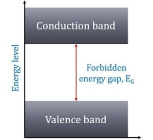
In terms of energy bands, it means that electrical conductors are those which have overlapping valence and conduction bands as shown in Fig (b).
In fact, there is no physical distinction between the two bands. Hence, the availability of a large number of conduction electrons.
Another point worth noting is that in the absence of forbidden energy gap in good conductors, there is no structure to establish holes.
The total current in such conductors is simply allowed of electrons. It is exactly for this reason that the existence of holes was not discovered until semiconductors were studied thoroughly.
Semiconductors
A semiconductor material is one whose electrical properties lie in between those of insulators and good conductors. Examples are germanium and silicon.
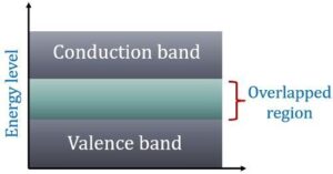
In terms of energy bands, semiconductors can be defined as those materials which have almost an empty conduction band and almost filled valence band with a very narrow energy gap (of the order of 1 eV) separating the two.
At 0°K, there are no electrons in the conduction band and the valence band is completely filled.
However, with an increase in temperature, the width of the forbidden energy bands is decreased so that some of the electrons are liberated into the conduction band.
In other words, the conductivity of semiconductors increases with temperature.
Moreover, such departing electrons leave behind positive holes in the valence band. Hence, the semiconductor current is the sum of electron and hole currents flowing in opposite directions.
Comparison between Conductor, Semiconductor and Insulator
| Parameter | Conductor | Semiconductor | Insulator |
|---|---|---|---|
| Forbidden energy gap | Not exist | Small (1 eV) | Large (>5 eV) |
| Conductivity | High (10-7 mho/m) | Medium (10-7 to 10-13 mho/m) | Very Low (10-3 mho/m) Almost negligible. |
| Resistivity | Low | Moderate | High |
| Flow of current | Due to movement of free electrons. | Due to movement of electrons and holes. | Almost negligible but only due to free electrons. |
| Temperature coefficient of resistance | Positive | Negative | Negative |
| Charge carriers in conduction band | Completely filled | Partially filled | Completely vacant |
| Charge carriers in valence band | Almost vacant | Partially filled | Completely filled |
| Example | Copper, Aluminium, graphite etc. | Silicon, Germanium, arsenic etc. | Paper, rubber, glass, plastic etc. |
| Applications | Conducting wires, Transformers, in electrical cords etc. | Diodes, transistors, optocouplers etc. | Sports equipment, home appliances etc. |


This is perfectly written and I completely agree!
this was great info!
good post
I don’t get it
loved it